The following is an analysis of its core features, advantages and disadvantages, and applicable scenarios:
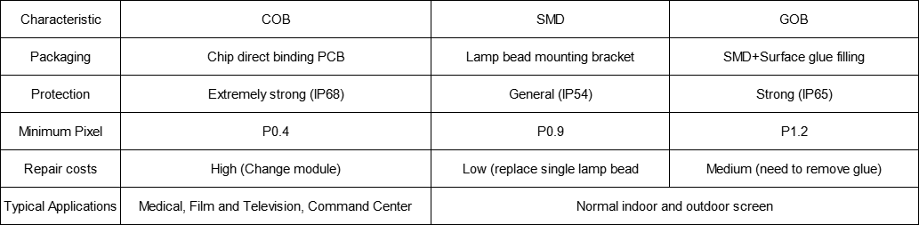
——COB vs SMD vs GOB comparison
——COB technology principle
1. Packaging process:
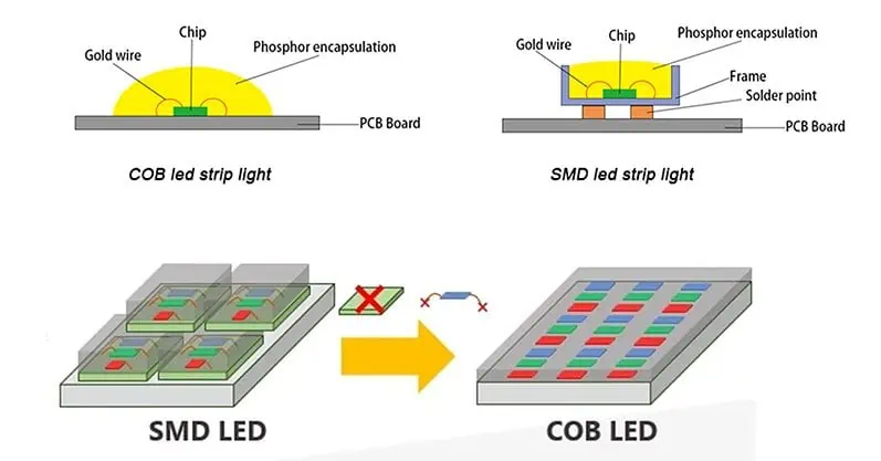
LED chip → die bonding (directly bonded to PCB) → wire bonding → fluorescent glue coating → overall packaging curing.
2. Structural features:
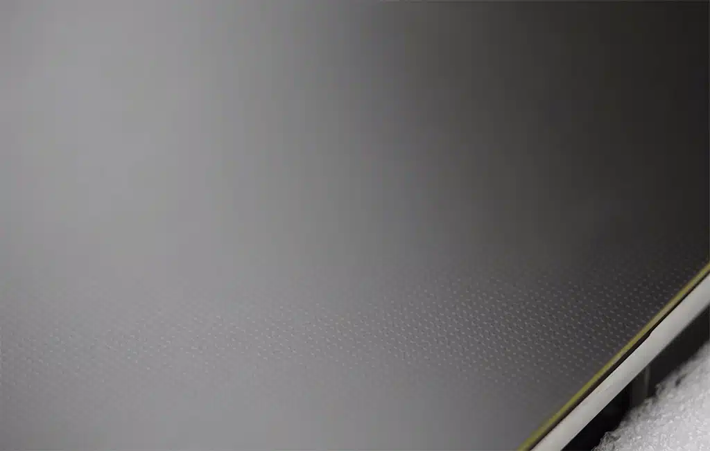
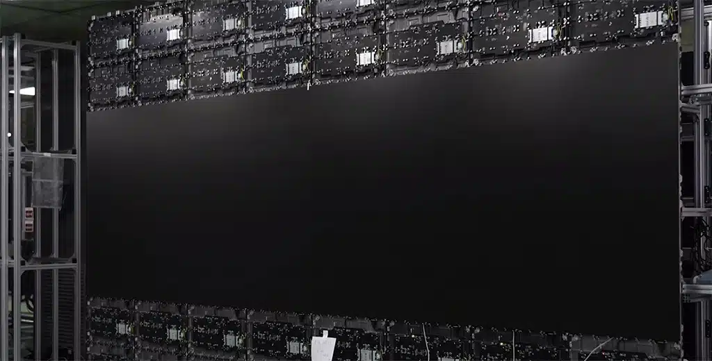
① No independent lamp beads, the chip is in direct contact with the PCB.
② The surface is covered with transparent or matte epoxy resin to form a flat and particle-free display surface.
——Total 5 advantages of COB LED display
1.Ultra-high reliability: no risk of lamp beads falling off, anti-vibration, anti-collision, protection level up to IP68 (underwater use)
2.Ultra-small pitch: mass production technology can reach P0.4 pitch, suitable for ultra-high-definition scenes such as medical imaging and command and control rooms.
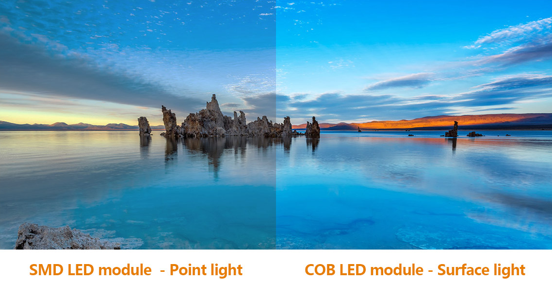
3.Extreme image quality: no pixel graininess, viewing angle 180°, contrast ratio > 10000:1 (pure black field, delicate bright part)
4.Long life: chip life > 100,000 hours (traditional SMD about 50,000 hours), slower light decay.
5. Environmental adaptability: moisture-proof, dust-proof, salt spray-resistant, suitable for harsh environments such as ships and mines.
—— 3 major disadvantages of COB LED display
1. High cost: The price is 2-3 times that of the same level SMD screen, mainly due to low yield rate (<90%) and process complexity.
2. Difficult maintenance: If a single chip is damaged, the entire module needs to be replaced, which is costly and time-consuming.
3. Brightness limitation: The current maximum brightness is about 2000cd/m², and outdoor applications require high-brightness optical films (such as brightness enhancement films)


 Sajja
Sajja